?2002 Microchip Technology Inc.
DS21462C-page 7
TC74
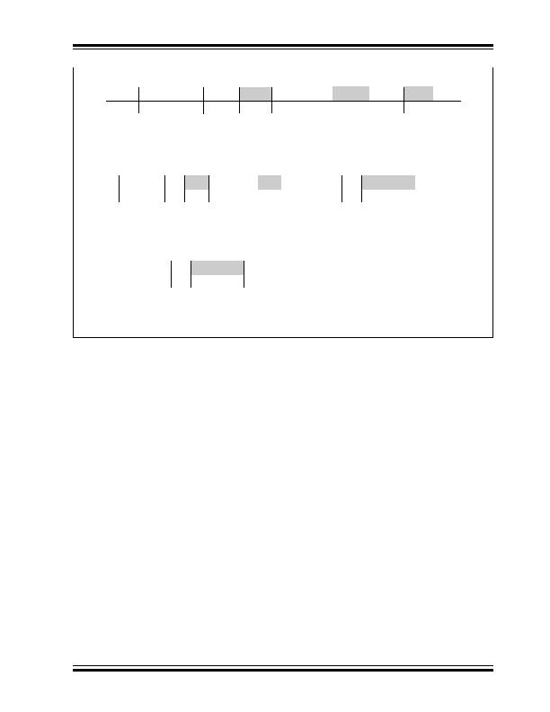
FIGURE 3-1:
SMBus/I
2
C Protocols.
3.3
START Condition (S)
The TC74 continuously monitors the SDA and SCLK
lines for a START condition (a high-to-low transition of
SDA while SCLK is high) and will not respond until this
condition is met.
3.4
Address Byte
Immediately following the START condition, the host
must transmit the address byte to the TC74. The states
of A2, A1 and A0 determine the SMBus/I
2
C address for
the TC74. The 7-bit address transmitted in the serial bit
stream must match for the TC74 to respond with an
Acknowledge (indicating the TC74 is on the bus and
ready to accept data). The 8-bit in the address byte is
a Read/Write bit. This bit is a 1 for a read operation or
0 for a write operation. During the first phase of any
transfer, this bit will be set = 0, indicating that the
command byte is being written.
3.5
Acknowledge (ACK)
Acknowledge (ACK) provides a positive handshake
between the host and the TC74. The host releases
SDA after transmitting 8 bits. The host then generates
a ninth clock cycle to allow the TC74 to pull the SDA
line low. This action acknowledges that the TC74
successfully received the previous 8 bits of data or
address.
3.6
Data Byte
After a successful ACK of the address byte, the host
must transmit the data byte to be written, or clock-in the
data to be read (see the appropriate timing diagrams).
ACK will be generated upon a successful write of a
data byte into the TC74.
3.7
STOP Condition (P)
Communications must be terminated by a STOP
condition (a low-to-high transition of SDA while SCLK
is high). The STOP condition must be communicated
by the transmitter to the TC74. Refer to Figure 1-1,
Timing Diagrams
, for serial bus timing.
S
Address
WR
ACK
Command
ACK
Data
ACK
P
8 Bits
7 Bits
8 Bits
Slave Address
Command Byte: selects
which register you are
writing to.
Data Byte: data goes
into the register set
by the command byte.
Write Byte Format
Read Byte Format
S
Address
WR
ACK
Command
ACK
S
Address
RD ACK Data NACK
P
7 Bits
8 Bits
7 Bits
8 Bits
Slave Address
Command Byte: selects
which register you are
reading from.
Slave Address: repeated
due to change in data-
flow direction.
Data Byte: reads from
the register set by the
command byte.
Receive Byte Format
S
Address
RD ACK Data
NACK P
7 Bits
8 Bits
Data Byte: reads data from
the register commanded by
the last Read Byte or Write
Byte transmission.
S = START Condition
P = STOP Condition
Shaded = Slave Transmission
发布紧急采购,3分钟左右您将得到回复。
相关PDF资料
TC77-5.0MOATR
IC THERMAL SENSOR SPI 5V 8-SOIC
TC9402EJD
IC V-FREQ/FREQ-V CONV 14CDIP
TCN75-5.0MUAG
IC TEMP SENSOR SRL 5.0V 8MSOP
TEA1750T/N1,518
IC PFC CONTROLLER DCM16SOIC
TEA1751T/N1,518
IC CTRLR GREENCHIP SMPS 16-SOIC
TEA1761T/N2,118
IC CTRLR GREENCHIP SYNC 8-SOIC
TEA1762T/N2/DG,118
IC CTLR SMPS SW SO14
TEA1791T/N1,118
IC CTRLR GREENCHIP SYNC 8-SOIC
相关代理商/技术参数
TC74A7-50VAT
制造商:MICROCHIP 制造商全称:Microchip Technology 功能描述:Tiny Serial Digital Thermal Sensor
TC74A7-50VCT
制造商:MICROCHIP 制造商全称:Microchip Technology 功能描述:Tiny Serial Digital Thermal Sensor
TC74AC00F
制造商:TOSHIBA 制造商全称:Toshiba Semiconductor 功能描述:QUAD 2 - INPUT NAND GATE
TC74AC00F(F)
制造商:Toshiba 功能描述:74AC Quad 2-Input NAND Gate 14SOP Bulk 制造商:Toshiba America Electronic Components 功能描述:IC, 74 series logic 制造商:Toshiba 功能描述:NAND Gate 4-Element 2-IN CMOS 14-Pin SOP Tube
TC74AC00F_12
制造商:TOSHIBA 制造商全称:Toshiba Semiconductor 功能描述:Quad 2-Input NAND Gate
TC74AC00FN
功能描述:IC GATE NAND QUAD 2INP 14-SOL RoHS:否 类别:集成电路 (IC) >> 逻辑 - 栅极和逆变器 系列:74AC 标准包装:2,000 系列:74LCX 逻辑类型:逆变器,缓冲器 电路数:1 输入数:8 特点:三态 电源电压:2 V ~ 3.6 V 电流 - 静态(最大值):10µA 输出电流高,低:24mA,24mA 逻辑电平 - 低:0.7 V ~ 0.8 V 逻辑电平 - 高:1.7 V ~ 2 V 额定电压和最大 CL 时的最大传播延迟:6.5ns @ 3.3V,50pF 工作温度:-40°C ~ 85°C 安装类型:表面贴装 供应商设备封装:20-SSOP 封装/外壳:20-SSOP(0.209",5.30mm 宽) 包装:带卷 (TR)
TC74AC00FN(ELF,M)
制造商:Toshiba America Electronic Components 功能描述:IC 2-INP NAND GATE QUAD 14-SOL 制造商:Toshiba America Electronic Components 功能描述:IC GATE NAND QUAD 2INP 14-SOL
TC74AC00FN(ELFM)
制造商:Toshiba America Electronic Components 功能描述:NAND Gate 4-Element 2-IN CMOS 14-Pin SOL T/R